Source: Agency for Science, Technology and Research (A*STAR), Singapore
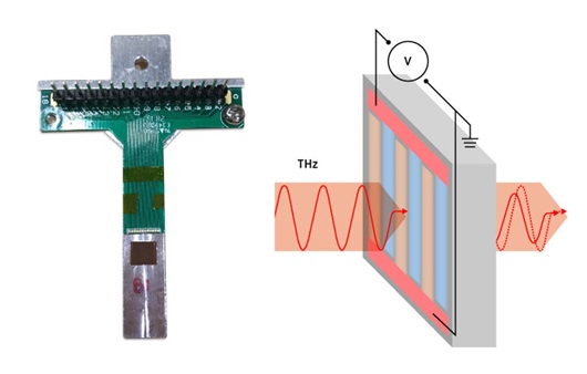
(left) A mounted device including the new tunable metasurface developed by Ding, Teng and co-workers. (right) When terahertz radiation hits the surface of interlinked p-type and n-type semiconducting silicon fingers, the amount of radiation reflected and transmitted can be controlled precisely using an applied voltage. Credit: A*STAR Institute of Materials Research and Engineering
The ability to manipulate light on a subwavelength-scale could lead to a revolution in photonic devices such as antennas, solar panels, and even cloaking devices. Nanotechnology advances have made this possible through the development of metasurfaces, materials covered in features smaller than the wavelength of the light.
Now, a team led by A*STAR researchers has produced a highly promising metasurface that can be precisely controlled using a conventional electrical circuit so that it reflects and transmits different amounts of radiation. It can even reach the condition of 'perfect antireflection' where it reflects no radiation at all. Specifically, the surface works with broadband terahertz radiation, which is found at the far end of the infrared spectrum and has many potential uses, particularly in security or medical fields.
"Terahertz radiation can penetrate a wide variety of non-conducting materials, but is blocked by liquid water or metals," explains Lu Ding, who led the work with Jinghua Teng at the A*STAR Institute of Materials Research and Engineering (IMRE). "This means that terahertz beams can be used for material characterization, layer inspection, and producing high-resolution images of the interior of solid objects. It is non-ionizing radiation, and safer than X-rays."
Previous metasurfaces have been designed to manipulate the reflection of terahertz radiation. However, their application has been limited, as Ding explains: "Conventional terahertz antireflection surfaces are passive and often employ an ultrathin metal coating that, once fabricated, becomes fixed and you can't actively tune its performance."
"An electrically tunable metasurface would produce more versatile devices and render more flexibility in system design," adds Teng. "It is the breakthrough the community is looking for."
Ding and Teng, along with coworkers at the A*STAR Institute of Microelectronics (IME), Nanyang Technological University, National University of Singapore and Jilin University in China, fabricated their new metasurface on a silicon wafer, using a process entirely compatible with the complementary metal¨Coxide semiconductor (CMOS) technologies that underpin most electronics.
The exposed metasurface contains stripes of semiconducting silicon, doped with other elements. These stripes are alternately n-type, in which the moving charge carriers are electrons, and p-type, in which the carriers are positively-charged 'holes' in the electron structure. When the voltage supplied to the p-n junctions is changed, the reflection and transmission of the radiation also change.
The team realized that the reflection coefficient increased in response to a temperature rise caused by the applied voltage. Meanwhile, the transmission showed a more complex response depending on the voltage polarity, which affected the type of charge carrier that became dominant. Using terahertz time-domain spectroscopy, the team showed that certain voltage conditions caused the echo pulse from the metasurface to vanish, representing complete antireflection.
As well as providing this unprecedented control over reflection and transmission, the metasurface has the benefit of being almost entirely flat at an atomic level. This makes it ideal for building up smooth layers in more complex devices.
"Another big advantage is for our research looking into how 2-D materials interact with 2-D metamaterials or metasurfaces, a topic in our project in A*STAR's 2-D Semiconductors Pharos Program," says Teng. "The atomically smooth surface makes the transfer and formation of 2-D-Si heterostructures much easier than the patterned surfaces of nano-sized pillars or disks seen on conventional metasurfaces."
"We could further exploit this type of metasurface by independently biasing the p-n junctions or designing modular functions, meaning that we would have pre-programmable metamaterials," says Ding. Teng adds that the same platform could be used for studying promising 2-D materials like molybdenum disulfide, which exhibits impressive electronic and optical properties for use in new flexible circuits.

 Copyright© 2006-2022 www.thznetwork.org.cn All Rights Reserved