by ICFO
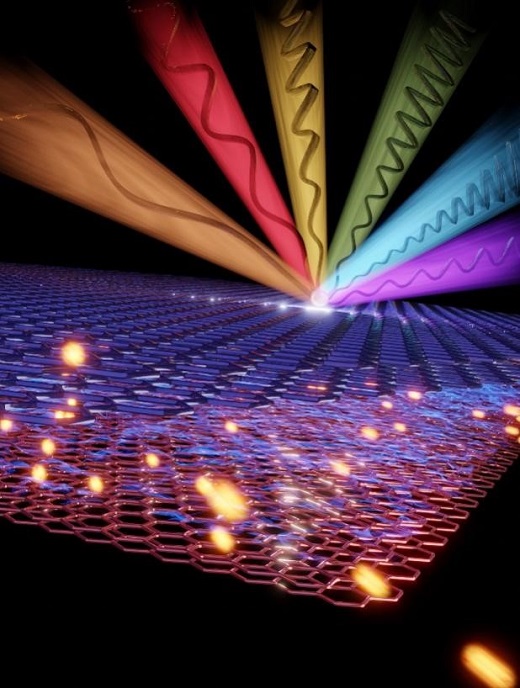
Artistic impression of a Twisted Double Bilayer Graphene device that is capable of detecting the entire light spectrum. Credit: ICFO/M. Ceccanti
Hyperspectral imaging uses the full spectrum of light to give detailed insights on nature and its behavior. These insights open a realm for manifold applications, including autonomous driving, environmental monitoring, health care, space exploration or even agriculture and food processing.
Imaging from the infrared to the terahertz regime poses a technological challenge because it requires devices that are efficient and sensitive enough over the entire range of the spectrum.
So far, the only ones that partially meet expectations are photoconductor arrays based on mercury cadmium telluride elements. Although this is the most suitable technology available currently, their performance efficiency in detecting light is not very broadband because they tend to be efficient absorbers for certain wavelengths but perform worse for others and they simply do not have the capabilities for detecting the longest wavelengths of light in the terahertz regime, which is becoming more and more relevant for technology.
As Frank Koppens, corresponding author of the study, mentions, "Twisting two-dimensional materials such as graphene has revolutionized the field of quantum materials, driven by the discovery of unconventional superconductivity. But recently, we have also been able to see that it's a platform for a wide range of applications, due to its unique and highly tunable properties."
Therefore, in the past years, bilayer graphene (BLG) has been shown to be an impressive photodetector when biased with external electric fields, although, because of its 2D nature, the light absorption is rather limited. Interestingly, BLG is compliant with the existing silicon technology, a must for being introduced to the market.
However, the need to apply electric field poses enormous difficulties in scaling up the fabrication in three dimensions, which would be necessary to overcome the problem of low absorption of BLG.
A new device
Twisted "double" bilayer graphene devices (TDBG), on the other hand, have emerged as a unique material that can avoid these restrictions. TDBG is made of two bilayer graphene stacks rotated or twisted by a large-angle (15 degrees) which have been recently shown to create their own intrinsic electric field without the need of extra electrodes that complicate the fabrication in case of BLG.
This has opened prospects of broadband detection in a scalable system, however, up to now, the light detection capabilities of TDBG have not been tested.
In a study published in Nature Photonics, researchers report on the development of a novel TDBG ultra-broadband photodetector capable of detecting light very efficiently in a spectral range that spans from the far-terahertz (100 μm wavelength, equivalent to 3 THz) all the way to near-infrared (2 μm wavelength or 150 THz) and with a good continuous efficiency in all the range, without any gaps.
The ICFO researchers Hitesh Agarwal & Krystian Nowakowski, were led by the postdoc researcher Dr. Roshan Krishna Kumar and ICREA Prof. at ICFO Frank Koppens. They worked in collaboration with ICREA Prof. Adrian Bachtold's group at ICFO, the group of prof. Giacomo Scalari from ETH Zurich, and researchers at University of Manchester, NIMS in Japan and CNRS in France.
The ultra-broadband photodetector has shown to have a good internal quantum efficiency, an enhancement of photoconductivity by interlayer screening, and scalability of TDBG because no gates are needed to apply the electric field in order to get the electronic bandgap.
In their experiment, the researchers carried out a thorough and comprehensible study of photoresponse in TDBG. They fabricated multiple devices of TDBG and studied their photoconductivity, i.e. how their electrical resistance changes under illumination.
As first co-author Krystian Nowakowski comments, "the idea of this experiment arose after reading a study in which researchers had found a small electronic bandgap in twisted double bilayer graphene (TDBG) without the need of applying an external electric field, that is usually necessary to open an electronic bandgap in the common one stack of bilayer graphene (BLG)."
"The presence of a bandgap makes bilayer graphene a good detector of light but the need to apply external electric field is a barrier for applications because of the complexity of scaling up the fabrication for industrial applications." After examining the literature, they saw that no one had ever tested this with "double" BLG, or TDBG.
So, the team put all their efforts into full motion to prepare the experiment. As Hitesh Agarwal, first co-author, recalls "making TDBG samples is not a trivial task. We started from exfoliating flakes of graphene, continuing this process until we could find a big enough flake of bilayer graphene. Then we cut the flake in half with a micromanipulator, pick up one of the halves, rotate it by 15 degrees and stack in onto the other to create a TDBG stack."
These devices were then cooled down to 4 kelvin temperature, to perform precise measurements of electrical resistance. Under illumination by mid-infrared light, they saw that the resistance dropped significantly, which prompted the possibility of utilizing these devices as photodetectors.
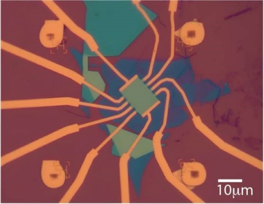
Optical image of a TDBG sample made into a Hall bar shape for precise measurement of electrical resistivity and photoconductivity. Credit: ICFO
Creativity in research
After several months of working intensively on the experiment, the team was obliged to search for logistics and experimental alternatives to overcome the restrictions imposed by the sudden shutdown in 2020 to continue the study, which included remote control of the equipment to continue measurements during pandemics.
The team worked arduous hours to setup the experiment, measure as much as possible to allow them to collect and understand the type of data that they were getting and what it actually meant. "One of the big challenges we faced was to actually understand the origin of the large response and benchmark it reliably with commercial technologies" recalls Roshan Krishna Kumar.
After many months of analyzing data, determining what had to be measured and why, learning how to distinguish between various hypotheses, and coming up with new ideas that could facilitate obtaining results, they were able to finally quantify the Internal Quantum Efficiency―indicator of the fraction of the absorbed photons that are converted into the measured change in electrical current―and found that the efficiency of most of the spectrum range was equal or above 40%, which is a good value and very promising when combined with the ultra-broad spectral range and scalability of TDBG.
Following the initial measurements, the researchers realized that the photodetector could have long-wavelength capabilities extending down to 2 THz after they characterized the intrinsic band gap of TDBG, which sets the cut-off frequency of their detectors.
Motivated by this tempting prospect, Hitesh Agarwal flew to Switzerland to perform measurements in the lab of Giacomo Scalari, who are experts in terahertz technologies and strong collaborators with ICFO under the project PhotoTBG. Using their customized broadband measurement set-ups, they demonstrated the ultrabroad wavelength range reported in the study.
The researchers then "focused on understanding the physical mechanism behind the measured signal. After long brainstorming with prof. Frank Koppens, we found that the response is mostly due to the photoconductive effect, where photons influence the resistance by creating more electron-hole pairs directly rather than the bolometric effect where photons heat the sample up and that indirectly influences the resistance by the change of temperature."
The results of this study show that the described methods and results can serve as a guide and a benchmark for other scientists using light for studying these very interesting twisted materials.
The explanation of conductivity enhancement by interlayer screening, the method to differentiate between bolometric and photoconductive response and the proposed idea of 3-dimensional stacking may well be used as a basis for further research on other two-dimensional materials.

 Copyright© 2006-2022 www.thznetwork.org.cn All Rights Reserved