by UCLA Engineering Institute for Technology Advancement
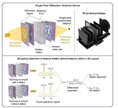
Illustration of a single-pixel diffractive terahertz sensor, which can detect hidden defects within 3D samples using a snapshot illumination, along with the photo of its 3D-printed prototype. Credit: Ozcan Lab @ UCLA.
In the realm of engineering and material science, detecting hidden structures or defects within materials is crucial. Traditional terahertz imaging systems, which rely on the unique property of terahertz waves to penetrate visibly opaque materials, have been developed to reveal the internal structures of various materials of interest.
This capability provides unprecedented advantages in numerous applications for industrial quality control, security screening, biomedicine, and defense. However, most existing terahertz imaging systems have limited throughput and bulky setups, and they need raster scanning to acquire images of the hidden features.
To change this paradigm, researchers at UCLA Samueli School of Engineering and the California NanoSystems Institute developed a unique terahertz sensor that can rapidly detect hidden defects or objects within a target sample volume using a single-pixel spectroscopic terahertz detector.
Instead of the traditional point-by-point scanning and digital image formation-based methods, this sensor inspects the volume of the test sample illuminated with terahertz radiation in a single snapshot, without forming or digitally processing an image of the sample.
Led by Dr. Aydogan Ozcan, the Chancellor's Professor of Electrical & Computer Engineering and Dr. Mona Jarrahi, the Northrop Grumman Endowed Chair at UCLA, this sensor serves as an all-optical processor, adept at searching for and classifying unexpected sources of waves caused by diffraction through hidden defects. The paper is published in the journal Nature Communications.
"It is a shift in how we view and harness terahertz imaging and sensing as we move away from traditional methods toward more efficient, AI-driven, all-optical sensing systems," said Dr. Ozcan, who is also the Associate Director of the California NanoSystems Institute at UCLA.
This new sensor comprises a series of diffractive layers, automatically optimized using deep learning algorithms. Once trained, these layers are transformed into a physical prototype using additive manufacturing approaches such as 3D printing. This allows the system to perform all-optical processing without the burdensome need for raster scanning or digital image capture/processing.
"It is like the sensor has its own built-in intelligence," said Dr. Ozcan, drawing parallels with their previous AI-designed optical neural networks. "Our design comprises several diffractive layers that modify the input terahertz spectrum depending on the presence or absence of hidden structures or defects within materials under test. Think of it as giving our sensor the capability to 'sense and respond' based on what it 'sees' at the speed of light."
To demonstrate their novel concept, the UCLA team fabricated a diffractive terahertz sensor using 3D printing and successfully detected hidden defects in silicon samples. These samples consisted of stacked wafers, with one layer containing defects and the other concealing them. The smart system accurately revealed the presence of unknown hidden defects with various shapes and positions.
The team believes their diffractive defect sensor framework can also work across other wavelengths, such as infrared and X-rays. This versatility heralds a plethora of applications, from manufacturing quality control to security screening and even cultural heritage preservation.
The simplicity, high throughput, and cost-effectiveness of this non-imaging approach promise transformative advances in applications where speed, efficiency, and precision are paramount.

 Copyright© 2006-2022 www.thznetwork.org.cn All Rights Reserved